Micron Shifts NAND Design to Bonded Wafers, Doubling Storage Density
The G11 generation moves memory arrays and logic onto separate wafers to reach 42 Gb/mm2 in late 2027.
By Alina Ndlovu ·
Micron Technology said this week it will begin ramping a new flash memory generation in the second half of 2027 that stores about twice as much data in the same silicon area as today's chips, a change that lowers the cost of high-capacity solid-state drives used in personal computers, data centers and AI systems.
The company said its current G9 generation stores about 21 Gb per square millimeter in triple-level-cell form. G11 reaches about 42 Gb/mm2. Micron also projects input and output speeds rising from 3,600 MT/s to as high as 5,400 MT/s, an increase of up to 50%, while the energy used to move each bit falls by more than 25%.
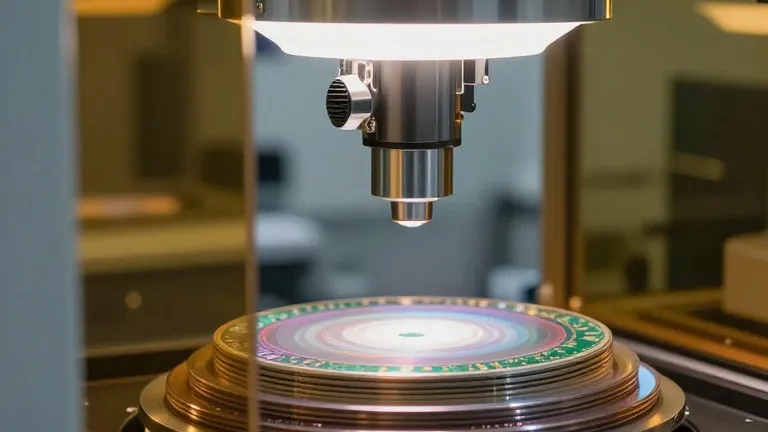
Micron has used CMOS-under-array designs for several generations of NAND. G11 introduces wafer-on-wafer bonding, which builds the memory array and the peripheral circuitry and input/output on separate wafers, each made with a process suited to its task, then bonds the two together. The same method is already used by China's YMTC.
Scott DeBoer, Micron's president and chief technology and products officer, said the company had committed to adopt the technique when it became cost-effective and matched product requirements. "This is the right timing for that technology," DeBoer said, calling G11 "the world's most advanced NAND" and confirming it relies on wafer-on-wafer bonding.
The G11 stack will exceed 400 layers. Micron has not disclosed the number of active wordline layers or memory decks, and it declined to provide architectural details for generations after G11. DeBoer said the company is working on high-mobility materials, denser cell structures and more energy-efficient data paths, and that both Micron and the industry continue to add layers and shrink cell dimensions.
Micron has not released production schedules or density targets for chips that follow G11. More technical details on the current generation are due in 2027, ahead of high-volume manufacturing.
Source: Tom's Hardware
More Business · Tech news · Rip-Off Report · Report a business · Got a Story?