SMIC and CXMT Face Rising Costs as DUV Lithography Replaces EUV
Multiple patterning allows Chinese chipmakers to produce advanced nodes, but the method increases defect risks and reduces yield per wafer.
By Jisoo Serrano ·
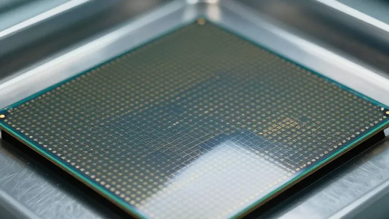
Chinese semiconductor manufacturers face a rising cost structure as they bypass the ban on extreme ultraviolet lithography equipment. Export controls have kept ASML's EUV machines out of the country, forcing domestic firms to rely on older deep ultraviolet tools. This reliance necessitates a technique called multiple patterning, which splits complex chip layers into simpler steps. While this method allows for the production of capable silicon, it introduces higher defect rates and longer production cycles.
The absence of EUV machinery remains the primary bottleneck for cutting-edge Chinese chip development. ASML holds the sole manufacturing capacity for these systems, which use 13.5 nanometer wavelength light to print fine features. Some analysts estimate the technological gap between China and Western rivals at five years or more. Despite this disparity, Chinese firms have achieved results that exceed initial expectations.
Evidence of this progress appeared in a 2023 teardown of the Huawei Mate 60 Pro. The analysis revealed that the Kirin 9000S processor was manufactured by SMIC using a second-generation 7 nanometer class process without EUV. More recent examinations of the Kirin 9030 suggest SMIC has moved its DUV-based process closer to 5 nanometer density levels. However, these processes still trail the leading technologies from TSMC and Samsung.
The core of this workaround is the splitting of design patterns. Instead of printing an intricate layer in a single pass, manufacturers build the intended layer step by step. Chris Mack, co-founder and CTO of Fractilia, noted that industry wisdom suggests three exposures on a 193 immersion tool cost about the same as one EUV exposure. At four masks, EUV becomes the cheaper option, making the DUV approach increasingly expensive as complexity rises.
Quality control presents another challenge. Each new pattern must align precisely with previous etching steps. More exposures lead to accumulated overlay errors and process variation. Designers often add space around features to compensate, which enlarges the chip and reduces the number of dies per wafer. Since wafers cost tens of thousands of dollars each, this reduction in yield represents a substantial financial loss. Mack emphasized that the market purchases die, not wafers.
Memory production illustrates the efficiency gap. A June report from Morgan Stanley estimated that CXMT, a Chinese DRAM maker, produces only about one-third as many bits per wafer as Western competitors. The bank described lithography access as a hard ceiling for Chinese memory development. Mack added that process node labels like 5 nanometer or 3 nanometer have limited meaning without context. He noted that SMIC's N+3 process, while a step forward, remains less scaled than established 5 nanometer processes from Samsung and TSMC.
DUV technology still offers some flexibility. Micron developed its 1-alpha DRAM without EUV, using multiple patterning and tight process control. Mack stated that Micron pushed 193 nanometer immersion technology farther than other memory manufacturers. Morgan Stanley considers CXMT's planned move to 1-alpha DRAM, intended for HBM3e, achievable without EUV. Douglas Fuller, a researcher at Copenhagen Business School, expects advanced packaging to allow firms to use DUV for the latest DRAM generations by the end of the decade.
Even Micron eventually adopted EUV for its 1-gamma DRAM. This generation delivers more than 30 percent greater bit density per wafer than the previous 1-beta generation. EUV has its own drawbacks, such as stochastic effects that require higher exposure doses. Mack said he would be hard pressed to believe a 3 nanometer or 2 nanometer node could be economically viable without EUV.
Source: Tom's Hardware